
Concepts
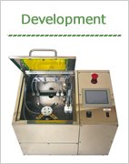
As a leading manufacturer of laboratory semiconductor manufacturing equipment, Photolithography.com can provide proven one-stop services regarding photolithography, including coating, exposure, development, and etching.
We have been developing various types of laboratory equipment since the 1960s. As a leading manufacturer, we take pride in our track record of delivering more than 7000 units to our customers. |
| ◆Delivery Record | |
| As a leading manufacturer of laboratory spin coaters and mask aligners, Photolithography.com (Mikasa) has delivered more than 7000 units to its customers. | |
| ◆ International Delivery Record | |
| China, Taiwan, South Korea, Singapore, Malaysia, India, Thailand, U.S.A., and Australia | |
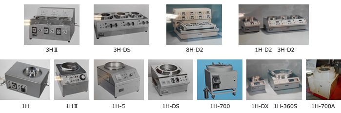
◆Previous Spin Coaters
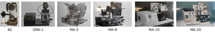
◆Previous Mask Aligners
We offer laboratory semiconductor manufacturing equipment used in the photolithography process, including coating, exposure, development, and etching, on a one-stop basis. |
 |
 |
 |
|
 |
|
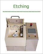 |
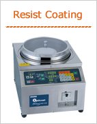
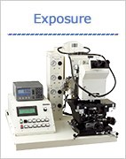
We offer all equipment required for the front-end stages of semiconductor manufacturing, including resist coating, exposure, development, and etching, on a one-stop basis. In addition.
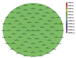
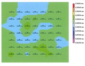
We have verification data on various coating materials to support your research. |
| (Coating) | ●We have verification data (coating thickness distribution) on various coating materials. |
| ●I have held a variety of test data. ・Thick coatings up to 100 μm thick can be formed. ・Coating thickness uniformity and more |
<Coating Thickness Distribution Data>
|
<Coating Thickness Distribution Data>
|
|
|
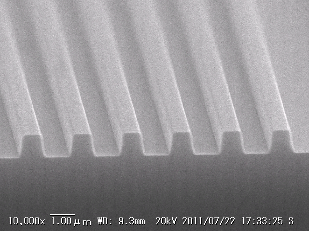
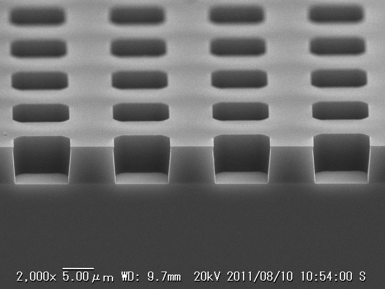
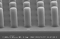
(Exposure)●We have a large database of verification data (resist patterns).
|
|
|
Our quality repair and maintenance services are available to support customers. |
◆Service networks in and outside Japan |
|
◆Repair and maintenance staff
◆ Technology and services (alternative units) | 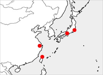 |